
Europe’s Chips Act Catch-Up Dilemma: The Gap Between Capacity Targets and Reality
Europe’s Chips Act was launched with a bold ambition: to roughly double the continent’s share of global semiconductor production and secure strategic autonomy in a technology that underpins everything from cars and industrial equipment to cloud computing and defense systems. Policymakers framed it as a catch‑up mechanism—Europe would move from dependence on foreign fabs toward a more balanced, resilient ecosystem.
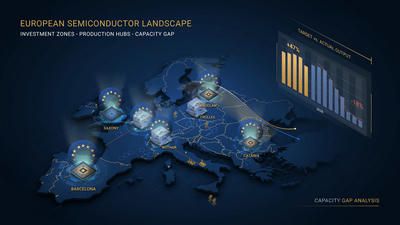
This article explores that catch‑up dilemma in depth: what Europe set out to achieve, how capacity targets stack up against actual fabs and projects, the structural reasons the gap persists, and what governments, companies, and investors can do to narrow it.
Europe’s Chips Act ambitions: targets and narrative
The European Chips Act crystallized a set of goals that had been evolving in policy circles for years. At its core was a quantitative target: significantly increasing Europe’s share of global semiconductor manufacturing by the early 2030s. The narrative emphasized resilience—avoiding a repeat of the pandemic‑era shortages that idled European car plants and exposed vulnerabilities in industrial supply chains. It also highlighted technological sovereignty, arguing that the continent needed domestic capacity not only in mature nodes for automotive and industrial use, but also in more advanced processes that support AI, high‑performance computing, and secure communications.
To translate ambitions into action, the Act bundled public subsidies, regulatory streamlining, and support for R&D and pilot lines. Member states layered their own programs on top, producing a patchwork of national incentives aimed at attracting fabs, packaging plants, and design centers. On PowerPoint slides and strategy documents, the map of planned capacity started to look crowded.
The reality check: what has actually materialized
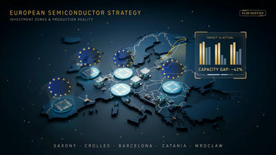
Despite an impressive pipeline of announcements, the hard reality of semiconductor projects has proved more stubborn. Building fabs and associated infrastructure is slow, capital‑intensive, and technologically demanding. Some high‑profile projects have moved forward, but many remain in early stages or have limited scope relative to global peers.
Several patterns stand out:
First, a relevant share of Europe’s new manufacturing capacity is concentrated in mature or specialty nodes rather than leading‑edge processes. These projects are important for automotive and industrial supply chains, but they do not radically change Europe’s position in the most advanced logic and memory segments.
Second, timelines have slipped. Environmental permitting, local infrastructure upgrades, workforce constraints, and supply of specialized equipment have often pushed completion dates further into the future. In some cases, announced capacity has yet to break ground or is still in the design phase.
Third, several flagship leading‑edge projects depend heavily on external partners—global chipmakers bringing their technology to Europe. This is strategically useful but also underscores that domestic technology bases in cutting‑edge nodes are still comparatively thin.
Why the gap persists: structural headwinds
The divergence between Europe’s Chips Act capacity targets and on‑the‑ground reality reflects a set of structural headwinds that are not easily overcome by subsidies alone.
Technology and experience gaps. Leading‑edge semiconductor manufacturing relies on decades of accumulated know‑how, process integration, and tacit experience. Regions that already host large advanced fabs have deep pools of specialized engineers, technicians, and supplier networks. Europe has strong strengths in equipment, some specialty manufacturing, and automotive‑grade semiconductors, but less native experience running large 3 nm or below logic lines at scale.
Capital intensity and risk appetite. Even with public support, advanced nodes and large fabs demand enormous private capital commitments. European industrial culture has often favored measured, incremental investments over the more aggressive, high‑risk capex cycles seen in some Asian and U.S. players. Bridging that difference takes more than grants—it requires boardroom conviction that returns justify the risk.
Fragmented policy landscape. The European Union sets broad frameworks, but member states manage their own incentives, regulations, and infrastructure. Coordination is improving, yet companies still face a mosaic of national rules, permitting timelines, and local conditions. This fragmentation can slow projects or complicate site selection, particularly for cross‑border ecosystems.
Workforce and ecosystem readiness. Semiconductor ecosystems depend on skilled workers, specialized suppliers, and supporting institutions. Europe has strong universities and precision industries, but scaling up enough fab‑ready operators, process engineers, and OSAT (assembly and test) capacity is a multi‑year project. Without those foundations, announced capacity can stay theoretical for longer than policymakers hope.
The mature‑node vs advanced‑node tension
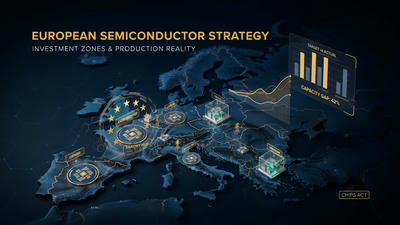
One of the clearest manifestations of Europe’s catch‑up dilemma lies in the tension between mature‑node priorities and advanced‑node ambitions.
On one hand, Europe has real strength and urgent need in mature nodes. Automotive, industrial automation, power electronics, and robust analog designs depend on processes that emphasize reliability, long lifecycles, and qualification rigor rather than the bleeding edge of transistor scaling. Investing in these areas is rational: it directly supports local industries and can quickly reduce vulnerability to imported supply shocks.
On the other hand, the global narrative of semiconductor competitiveness is increasingly driven by advanced nodes, AI accelerators, and high‑performance computing. Without a credible footprint in sub‑5 nm logic and advanced packaging, Europe risks remaining peripheral in the most dynamic segments of the industry, relying on imported chips for strategic workloads even as it builds strong capabilities for cars and factories.
The Chips Act tries to straddle both worlds, but finite capital and limited industrial capacity make it challenging to fully satisfy each. The result is that mature‑node capacity is more visibly progressing, while advanced‑node ambitions largely depend on foreign partners and long‑term aspirations.
Packaging, equipment, and materials: the quieter but critical layers
Another facet of the gap between targets and reality lies in the quieter layers of the semiconductor stack—advanced packaging, equipment, and materials.
Europe is home to leading equipment firms in lithography and other tool segments, as well as strong materials producers for certain chemicals and substrates. However, translating these strengths into integrated regional ecosystems requires deliberate design. Advanced packaging, in particular, has become a strategic bottleneck worldwide as chipmakers embrace chiplets, 2.5D and 3D integration, and HBM‑class memory systems.
Capacity targets often focus on wafer output, but system performance increasingly depends on where and how chips are packaged and tested. Europe’s challenge is to ensure that new fab projects are matched by adequate downstream capacity: OSATs, packaging houses, substrate and interposer producers, and test infrastructure capable of handling advanced designs. Without that, wafers may still need to travel abroad for final integration, limiting the resilience benefits of domestic manufacturing.
Timing and global cycles: racing against moving targets
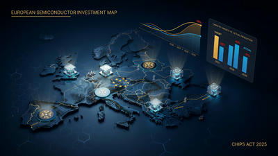
The semiconductor industry does not stand still while Europe builds fabs. Global leaders continue to ramp new nodes, invest in more advanced packaging, and expand capacity in regions with established ecosystems. This creates a moving target problem: by the time a new European fab comes online at a certain node, the global frontier may have moved ahead, shifting competitive benchmarks.
This doesn’t invalidate Europe’s efforts—mature and mid‑range nodes will remain important—but it complicates the catch‑up narrative. Capacity targets set years in advance may need revision as technology roadmaps evolve, particularly around AI training workloads, edge compute, and networking silicon. The risk is that Europe finally “catches up” to a point that the market has partly moved past, unless projects are designed with clear upgrade paths and forward‑compatible infrastructure.
Implications for European industry and investors
The gap between capacity targets and reality has tangible consequences for companies and investors operating in Europe.
For European industrial incumbents—automotive, machinery, robotics, energy—pragmatic sourcing strategies remain essential. Even as new local capacity emerges, these firms must maintain diversified global relationships for critical chips, while selectively anchoring long‑term supply agreements with European fabs where it makes economic and strategic sense.
For semiconductor companies and startups, the Chips Act creates opportunities but also competition and complexity. Domestic firms can tap subsidies to expand capacity, invest in specialty products, or collaborate with R&D institutions. Yet they also face the reality of competing with global giants who may establish local fabs under the same policy umbrella. Carefully chosen niches—power electronics, automotive‑grade semis, sensors, analog—and strong partnerships may matter more than trying to match global leaders across the board.
Investors, meanwhile, must separate signal from noise. Not every announced project will deliver on time or at the promised scale. The most compelling investment cases will likely be those with clear private‑sector economics, strong management, robust ecosystem support, and realistic node choices, rather than those relying solely on subsidy narratives.
What Europe can do to narrow the gap
The catch‑up dilemma is not insurmountable. Several strategic adjustments could help bring capacity targets closer to reality over time.
Deepen ecosystem planning, not just fab counts. Policymakers and industry groups can move beyond counting planned wafers to mapping full ecosystems: equipment, packaging, materials, talent, and logistics. Coordinated planning around regional clusters can ensure that each new fab is backed by complementary capabilities.
Streamline permitting and infrastructure delivery. Environmental and construction approvals must remain rigorous, but they can be made more predictable and timely through standardized processes, dedicated industrial zones, and early coordination between public authorities and project sponsors.
Invest in talent pipelines. Scaling semiconductor capacity requires technicians, engineers, and specialized managers. Europe can expand vocational programs, university‑industry partnerships, and cross‑border mobility schemes to build a deeper pool of semiconductor‑literate workers.
Prioritize upgradeable platforms. When Europe backs new fabs or packaging plants, designing them as upgradeable platforms—able to move from one node or packaging generation to the next with incremental investment—reduces the risk that capacity becomes obsolete as global technology advances.
Support strategic partnerships without over‑reliance. Collaborations with global chipmakers bring valuable technology and experience. Europe can structure these partnerships to maximize local capability transfer while still nurturing domestic firms that can grow into competitive suppliers.
Balancing realism and ambition
Europe’s Chips Act reflects both a justified concern about semiconductor dependence and a healthy ambition to play a stronger role in a critical global industry. The catch‑up dilemma arises when aspirations outpace the practical speed of building fabs, ecosystems, and talent. Recognizing that gap does not mean abandoning the project; rather, it calls for soberer, more granular strategy.
Realistic planning means accepting that Europe will likely remain deeply connected to global semiconductor networks, even as it builds more capacity at home. It means shaping targets around specific strengths—automotive, industrial, power, certain equipment and materials—while making targeted bets where advanced capacity can be competitive and sustainable. And it means emphasizing resilience and capability over symbolic metrics, focusing on whether European industry can access the chips it needs reliably, even if the continent never dominates global wafer statistics.
Ultimately, the success of Europe’s Chips Act will be judged less by headline capacity numbers than by whether European companies find themselves better insulated from future shocks, more capable of innovating on top of local ecosystems, and more confident participating in the global semiconductor economy. Bridging the gap between capacity targets and reality is a long‑term project—but acknowledging the dilemma clearly is the first step in resolving it.





